- 您现在的位置:买卖IC网 > Sheet目录3881 > PIC18F6525T-I/PT (Microchip Technology)IC PIC MCU FLASH 24KX16 64TQFP
PIC18F6525/6621/8525/8621
DS39612B-page 116
2005 Microchip Technology Inc.
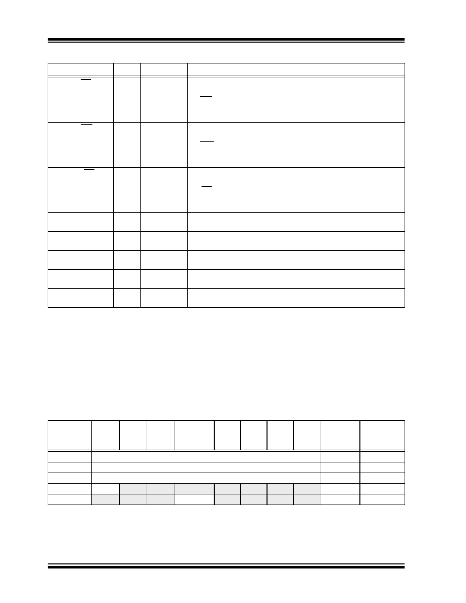
TABLE 10-9:
PORTE FUNCTIONS
TABLE 10-10: SUMMARY OF REGISTERS ASSOCIATED WITH PORTE
Name
Bit#
Buffer Type
Function
RE0/AD8/RD/P2D
bit 0
ST/TTL(1)
Input/output port pin, address/data bit 8, read control for Parallel Slave
Port or Enhanced PWM 2 output P2D
For RD (PSP Control mode):
1
= Not a read operation
0
= Read operation, reads PORTD register (if chip selected)
RE1/AD9/WR/P2C
bit 1
ST/TTL(1)
Input/output port pin, address/data bit 9, write control for Parallel Slave
Port or Enhanced PWM 2 output P2C
For WR (PSP Control mode):
1
= Not a write operation
0
= Write operation, writes PORTD register (if chip selected)
RE2/AD10/CS/P2B
bit 2
ST/TTL(1)
Input/output port pin, address/data bit 10, chip select control for
Parallel Slave Port or Enhanced PWM 2 output P2B
For CS (PSP Control mode):
1
= Device is not selected
0
= Device is selected
RE3/AD11/P3C(2)
bit 3
ST/TTL(1)
Input/output port pin, address/data bit 11 or Enhanced PWM 3
output P3C.
RE4/AD12/P3B(2)
bit 4
ST/TTL(1)
Input/output port pin, address/data bit 12 or Enhanced PWM 3
output P3B.
RE5/AD13/P1C(2)
bit 5
ST/TTL(1)
Input/output port pin, address/data bit 13 or Enhanced PWM 1
output P1C.
RE6/AD14/P1B(2)
bit 6
ST/TTL(1)
Input/output port pin, address/data bit 14 or Enhanced PWM 1
output P1B.
RE7/AD15/
ECCP2(3)/P2A(3)
bit 7
ST/TTL(1)
Input/output port pin, address/data bit 15, Enhanced Capture 2 input/
Compare 2 output/PWM 2 output or Enhanced PWM 2 output P2A.
Legend: ST = Schmitt Trigger input, TTL = TTL input
Note 1:
Input buffers are Schmitt Triggers when in I/O or CCP/ECCP modes and TTL buffers when in System Bus
or PSP Control modes.
2:
Valid for all PIC18F6525/6621 devices and PIC18F8525/8621 devices when ECCPMX is set. Alternate
assignments for P1B/P1C/P3B/P3C are RH7, RH6, RH5 and RH4, respectively.
3:
Valid for all PIC18F6525/6621 devices and PIC18F8525/8621 devices in Microcontroller mode when
CCP2MX is not set. RC1 is the default assignment for ECCP2/P2A for all devices in Microcontroller mode
when CCP2MX is set; RB3 is the alternate assignment for PIC18F8525/8621 devices in operating modes
except Microcontroller mode when CCP2MX is not set.
Name
Bit 7
Bit 6
Bit 5
Bit 4
Bit 3
Bit 2
Bit 1
Bit 0
Value on:
POR, BOR
Value on
all other
Resets
TRISE
PORTE Data Direction Control Register
1111 1111
PORTE
Read PORTE pin/Write PORTE Data Latch
xxxx xxxx
uuuu uuuu
LATE
Read PORTE Data Latch/Write PORTE Data Latch
xxxx xxxx
uuuu uuuu
MEMCON(1)
EBDIS
—
WAIT1
WAIT0
—
WM1
WM0
0-00 --00
0000 --00
PSPCON(2)
IBF
OBF
IBOV
PSPMODE
—
0000 ----
Legend: x = unknown, u = unchanged, — = unimplemented, read as ‘0’. Shaded cells are not used by PORTE.
Note 1:
This register is unused on PIC18F6525/6621 devices and reads as ‘0’.
2:
Enabled only in Microcontroller mode for PIC18F8525/8621 devices.
发布紧急采购,3分钟左右您将得到回复。
相关PDF资料
PIC18F4439-E/ML
IC PIC MCU FLASH 6KX16 44QFN
XF2J-2024-11
CONN FPC 20POS 0.5MM SMT
PIC16LF747-I/ML
IC PIC MCU FLASH 4KX14 44QFN
XF2J-1824-11
CONN FPC 18POS 0.5MM SMT
XF2J-1624-11
CONN FPC 16POS 0.5MM SMT
XF2J-1424-11
CONN FPC 14POS 0.5MM SMT
XF2J-1224-11
CONN FPC 12POS 0.5MM SMT
XF2J-1024-11
CONN FPC 10POS 0.5MM SMT
相关代理商/技术参数
PIC18F6527-I/PT
功能描述:8位微控制器 -MCU 48 KB FL 4K RAM 70 I/O RoHS:否 制造商:Silicon Labs 核心:8051 处理器系列:C8051F39x 数据总线宽度:8 bit 最大时钟频率:50 MHz 程序存储器大小:16 KB 数据 RAM 大小:1 KB 片上 ADC:Yes 工作电源电压:1.8 V to 3.6 V 工作温度范围:- 40 C to + 105 C 封装 / 箱体:QFN-20 安装风格:SMD/SMT
PIC18F6527-I/PT
制造商:Microchip Technology Inc 功能描述:8-Bit Microcontroller IC
PIC18F6527T-I/PT
功能描述:8位微控制器 -MCU 48 KB FL 4K RAM 70 I/O RoHS:否 制造商:Silicon Labs 核心:8051 处理器系列:C8051F39x 数据总线宽度:8 bit 最大时钟频率:50 MHz 程序存储器大小:16 KB 数据 RAM 大小:1 KB 片上 ADC:Yes 工作电源电压:1.8 V to 3.6 V 工作温度范围:- 40 C to + 105 C 封装 / 箱体:QFN-20 安装风格:SMD/SMT
PIC18F6585-E/L
功能描述:8位微控制器 -MCU 48KB 3328 RAM 52 I/O RoHS:否 制造商:Silicon Labs 核心:8051 处理器系列:C8051F39x 数据总线宽度:8 bit 最大时钟频率:50 MHz 程序存储器大小:16 KB 数据 RAM 大小:1 KB 片上 ADC:Yes 工作电源电压:1.8 V to 3.6 V 工作温度范围:- 40 C to + 105 C 封装 / 箱体:QFN-20 安装风格:SMD/SMT
PIC18F6585-E/PT
功能描述:8位微控制器 -MCU 48KB 3328 RAM 52 I/O RoHS:否 制造商:Silicon Labs 核心:8051 处理器系列:C8051F39x 数据总线宽度:8 bit 最大时钟频率:50 MHz 程序存储器大小:16 KB 数据 RAM 大小:1 KB 片上 ADC:Yes 工作电源电压:1.8 V to 3.6 V 工作温度范围:- 40 C to + 105 C 封装 / 箱体:QFN-20 安装风格:SMD/SMT
PIC18F6585-I/L
功能描述:8位微控制器 -MCU 48KB 3328 RAM 52 I/O RoHS:否 制造商:Silicon Labs 核心:8051 处理器系列:C8051F39x 数据总线宽度:8 bit 最大时钟频率:50 MHz 程序存储器大小:16 KB 数据 RAM 大小:1 KB 片上 ADC:Yes 工作电源电压:1.8 V to 3.6 V 工作温度范围:- 40 C to + 105 C 封装 / 箱体:QFN-20 安装风格:SMD/SMT
PIC18F6585-I/L
制造商:Microchip Technology Inc 功能描述:8-Bit Microcontroller IC
PIC18F6585-I/PT
功能描述:8位微控制器 -MCU 48KB 3328 RAM 52 I/O RoHS:否 制造商:Silicon Labs 核心:8051 处理器系列:C8051F39x 数据总线宽度:8 bit 最大时钟频率:50 MHz 程序存储器大小:16 KB 数据 RAM 大小:1 KB 片上 ADC:Yes 工作电源电压:1.8 V to 3.6 V 工作温度范围:- 40 C to + 105 C 封装 / 箱体:QFN-20 安装风格:SMD/SMT